


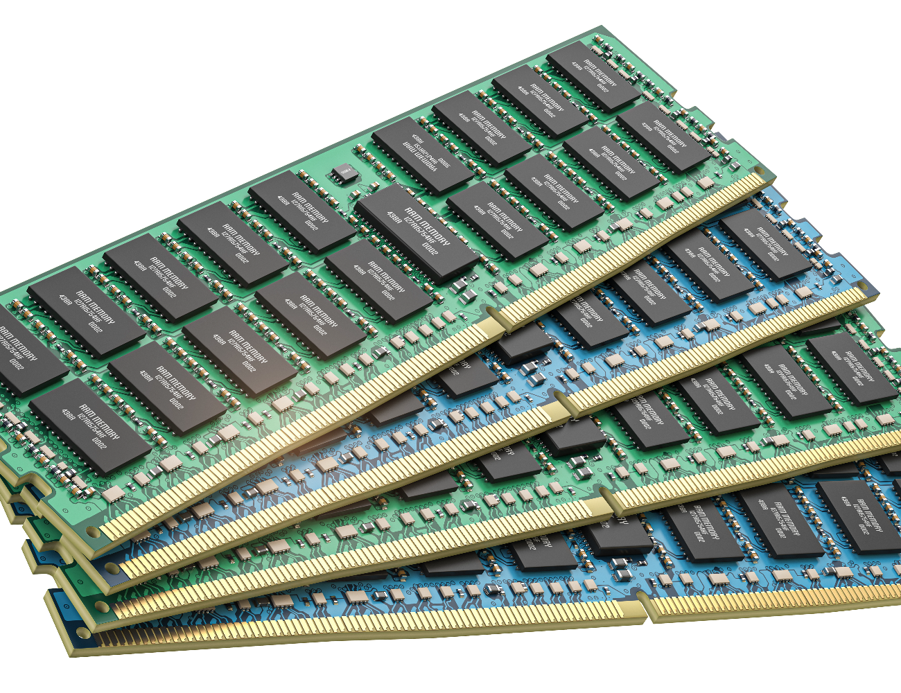
Printed circuit boards are the backbone of modern electronics, providing the essential pathways that allow components to communicate. For applications that require a balance between complexity, performance, and cost-efficiency, Dual Layer PCB Solutions stand out as the preferred choice. Offering high-quality fabrication and assembly, these boards meet the demands of countless industries, from consumer devices to industrial systems.
Understanding the Advantages of Two-Sided PCB Technology
Two-sided printed circuit boards allow components and copper traces to be placed on both the top and bottom layers, significantly increasing design flexibility. Dual Layer PCB Solutions are ideal when single-layer boards cannot provide enough routing options for more complex circuits but a multi-layer option would be excessive or too costly. This design strikes the perfect balance, delivering higher functionality without unnecessary manufacturing expense.
Meeting the Needs of Diverse Applications
From LED lighting systems and power supplies to automotive electronics and industrial controls, Dual Layer PCB Solutions support a wide range of uses. The ability to mount components on both sides enhances circuit density while maintaining a manageable board size. This is particularly valuable for products that must remain compact yet highly functional, allowing engineers to maximize performance within tight design constraints.
Precision Fabrication for Reliable Performance
The manufacturing process for Dual Layer PCB Solutions requires precision at every stage. Advanced drilling and plating techniques ensure strong via connections between the two layers, while high-quality copper cladding supports consistent conductivity. Careful attention to solder mask application, surface finishing, and quality control guarantees that each board meets the highest performance standards.
Material Selection for Durability and Function
Choosing the right materials is crucial to achieving reliable results. A professional provider of Dual Layer PCB Solutions uses premium substrates such as FR-4, high-Tg laminates, and specialized heat-resistant materials depending on the application. These materials not only improve electrical performance but also enhance thermal stability, ensuring that the boards operate effectively even in demanding environments.
Supporting Both Prototype and Mass Production
Whether developing a new product concept or scaling up for mass manufacturing, Dual Layer PCB Solutions can be adapted to fit the project’s needs. Rapid prototyping capabilities allow designers to test and refine their circuits quickly, while scalable production ensures that large orders maintain consistent quality from the first board to the last.
Quality Assurance Through Rigorous Testing
Reliable performance is achieved through stringent inspection and testing procedures. High-quality Dual Layer PCB Solutions undergo electrical testing to verify continuity, isolation, and signal integrity. Automated optical inspection ensures precise component placement and accurate soldering, reducing the risk of defects and increasing long-term dependability.
Cost-Effective Versatility
One of the reasons Dual Layer PCB Solutions are so popular is their ability to deliver enhanced circuit complexity without the expense of multi-layer manufacturing. This makes them a cost-effective choice for many applications, providing excellent value without sacrificing quality or performance. Businesses can achieve better functionality while keeping production budgets under control.
Driving Innovation in Product Design
The flexibility offered by Dual Layer PCB Solutions empowers engineers to create more advanced, compact, and efficient products. By enabling better component layout and more efficient routing, these boards open the door to innovation in consumer electronics, telecommunications, renewable energy systems, and beyond. As technology advances, their importance in bridging design efficiency and cost-effectiveness continues to grow.